- 您现在的位置:买卖IC网 > Sheet目录3841 > PIC16C63A-04I/SO (Microchip Technology)IC MCU OTP 4KX14 PWM 28SOIC
PIC16C63A/65B/73B/74B
DS30605C-page 14
2000 Microchip Technology Inc.
3.1
Clocking Scheme/Instruction
Cycle
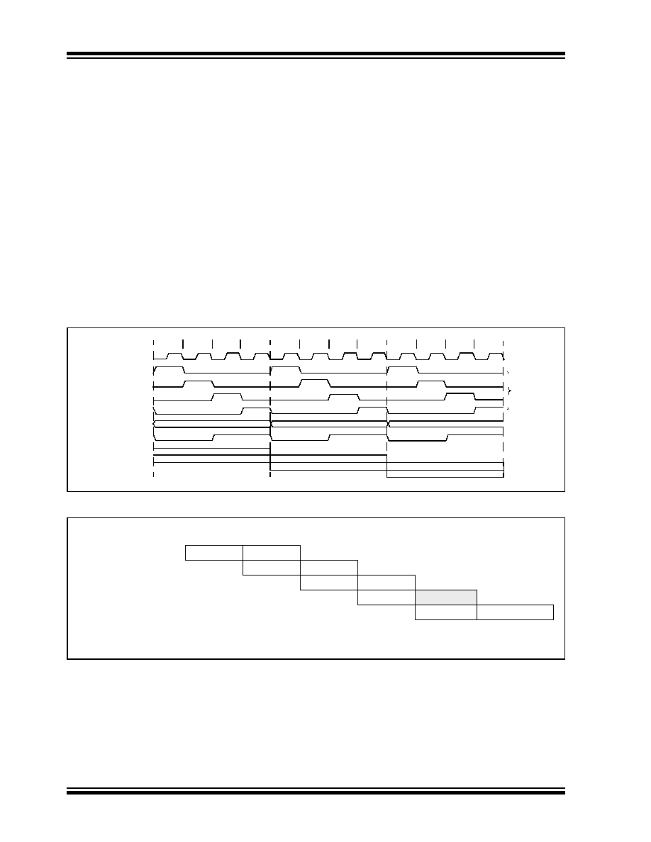
The clock input (from OSC1) is internally divided by
four to generate four non-overlapping quadrature
clocks, namely Q1, Q2, Q3 and Q4. Internally, the pro-
gram counter (PC) is incremented every Q1, the
instruction is fetched from the program memory and
latched into the instruction register in Q4. The instruc-
tion is decoded and executed during the following Q1
through Q4. The clocks and instruction execution flow
is shown in Figure 3-2.
3.2
Instruction Flow/Pipelining
An “Instruction Cycle” consists of four Q cycles (Q1,
Q2, Q3 and Q4). The instruction fetch and execute are
pipelined such that fetch takes one instruction cycle,
while decode and execute takes another instruction
cycle. However, due to the pipelining, each instruction
effectively executes in one cycle. If an instruction
causes the program counter to change (e.g., GOTO),
then two cycles are required to complete the instruction
A fetch cycle begins with the program counter (PC)
incrementing in Q1.
In the execution cycle, the fetched instruction is latched
into the “Instruction Register" (IR) in cycle Q1. This
instruction is then decoded and executed during the
Q2, Q3 and Q4 cycles. Data memory is read during Q2
(operand read) and written during Q4 (destination
write).
FIGURE 3-2:
CLOCK/INSTRUCTION CYCLE
EXAMPLE 3-1:
INSTRUCTION PIPELINE FLOW
Q1
Q2
Q3
Q4
Q1
Q2
Q3
Q4
Q1
Q2
Q3
Q4
OSC1
Q1
Q2
Q3
Q4
PC
OSC2/CLKOUT
(RC mode)
PC
PC+1
PC+2
Fetch INST (PC)
Execute INST (PC-1)
Fetch INST (PC+1)
Execute INST (PC)
Fetch INST (PC+2)
Execute INST (PC+1)
Internal
phase
clock
Note:
All instructions are single cycle, except for any program branches. These take two cycles, since the fetch instruction is
“flushed” from the pipeline, while the new instruction is being fetched and then executed.
TCY0TCY1TCY2TCY3TCY4TCY5
1. MOVLW 55h
Fetch 1
Execute 1
2. MOVWF PORTB
Fetch 2
Execute 2
3. CALL
SUB_1
Fetch 3
Execute 3
4. BSF
PORTA, BIT3 (Forced NOP)
Fetch 4
Flush
5. Instruction @ address SUB_1
Fetch SUB_1 Execute SUB_1
发布紧急采购,3分钟左右您将得到回复。
相关PDF资料
52559-2270
CONN FFC 22POS .5MM VERT ZIF SMD
52559-1870
CONN FFC 18POS .5MM VERT ZIF SMD
DSPIC33EP64MC506-I/PT
IC DSC 16BIT 64KB FLASH 64TQFP
52745-1896
CONN FFC 18POS .5MM R/A ZIF SMD
PIC16LC622-04/P
IC MCU OTP 2KX14 COMP 18DIP
PIC16LF84A-04/P
IC MCU FLASH 1KX14 EE 18DIP
DSPIC30F1010-30I/MM
IC DSPIC MCU/DSP 6K 28QFN
52745-1696
CONN FFC 16POS .5MM R/A ZIF SMD
相关代理商/技术参数
PIC16C63A-04I/SP
功能描述:8位微控制器 -MCU 7KB 192 RAM 22 I/O RoHS:否 制造商:Silicon Labs 核心:8051 处理器系列:C8051F39x 数据总线宽度:8 bit 最大时钟频率:50 MHz 程序存储器大小:16 KB 数据 RAM 大小:1 KB 片上 ADC:Yes 工作电源电压:1.8 V to 3.6 V 工作温度范围:- 40 C to + 105 C 封装 / 箱体:QFN-20 安装风格:SMD/SMT
PIC16C63A-04I/SS
功能描述:8位微控制器 -MCU 7KB 192 RAM 22 I/O RoHS:否 制造商:Silicon Labs 核心:8051 处理器系列:C8051F39x 数据总线宽度:8 bit 最大时钟频率:50 MHz 程序存储器大小:16 KB 数据 RAM 大小:1 KB 片上 ADC:Yes 工作电源电压:1.8 V to 3.6 V 工作温度范围:- 40 C to + 105 C 封装 / 箱体:QFN-20 安装风格:SMD/SMT
PIC16C63A04SP
制造商:MICROCHIP 功能描述:NEW
PIC16C63A-20/SO
功能描述:8位微控制器 -MCU 7KB 192 RAM 22 I/O RoHS:否 制造商:Silicon Labs 核心:8051 处理器系列:C8051F39x 数据总线宽度:8 bit 最大时钟频率:50 MHz 程序存储器大小:16 KB 数据 RAM 大小:1 KB 片上 ADC:Yes 工作电源电压:1.8 V to 3.6 V 工作温度范围:- 40 C to + 105 C 封装 / 箱体:QFN-20 安装风格:SMD/SMT
PIC16C63A-20/SP
功能描述:8位微控制器 -MCU 7KB 192 RAM 22 I/O RoHS:否 制造商:Silicon Labs 核心:8051 处理器系列:C8051F39x 数据总线宽度:8 bit 最大时钟频率:50 MHz 程序存储器大小:16 KB 数据 RAM 大小:1 KB 片上 ADC:Yes 工作电源电压:1.8 V to 3.6 V 工作温度范围:- 40 C to + 105 C 封装 / 箱体:QFN-20 安装风格:SMD/SMT
PIC16C63A-20/SP
制造商:Microchip Technology Inc 功能描述:8 Bit Microcontroller Clock Speed:20MHz
PIC16C63A-20/SS
功能描述:8位微控制器 -MCU 7KB 192 RAM 22 I/O RoHS:否 制造商:Silicon Labs 核心:8051 处理器系列:C8051F39x 数据总线宽度:8 bit 最大时钟频率:50 MHz 程序存储器大小:16 KB 数据 RAM 大小:1 KB 片上 ADC:Yes 工作电源电压:1.8 V to 3.6 V 工作温度范围:- 40 C to + 105 C 封装 / 箱体:QFN-20 安装风格:SMD/SMT
PIC16C63A-20E/SO
功能描述:8位微控制器 -MCU 7KB 192 RAM 22 I/O RoHS:否 制造商:Silicon Labs 核心:8051 处理器系列:C8051F39x 数据总线宽度:8 bit 最大时钟频率:50 MHz 程序存储器大小:16 KB 数据 RAM 大小:1 KB 片上 ADC:Yes 工作电源电压:1.8 V to 3.6 V 工作温度范围:- 40 C to + 105 C 封装 / 箱体:QFN-20 安装风格:SMD/SMT